Multilayer PCB
Orbis Electrica designs and manufactures Multilayer Printed Circuit Boards (PCBs) for modern electronic systems that demand high circuit density, signal integrity, and long-term reliability. By stacking multiple conductive and insulating layers into a single board, multilayer PCBs enable complex functionality in compact form factors while maintaining excellent electrical and thermal performance. These boards are ideally suited to high-speed digital, RF, mixed-signal, and power-sensitive applications where layout discipline and stack-up design are critical to system success.
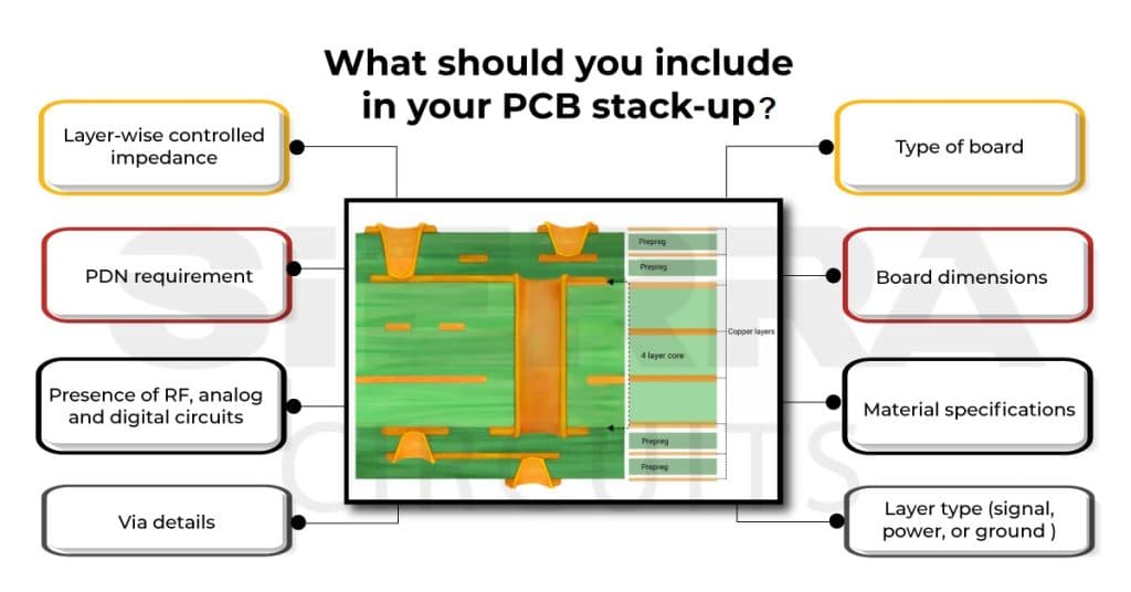
What Is a Multilayer PCB?
A multilayer PCB consists of three or more copper layers separated by insulating dielectric material and bonded together through a controlled lamination process. Internal layers are commonly dedicated to solid power and ground planes, while outer layers route high-speed and low-speed signals. This layered construction enables controlled impedance routing, reduced electromagnetic interference (EMI), improved return paths, and higher component density compared with single- or double-sided PCBs.
Key Benefits
High Component Density
Multiple internal layers allow complex circuitry and higher component counts to be implemented without increasing board size, supporting compact and feature-rich designs.
Enhanced Signal Integrity
Dedicated power and ground planes provide stable reference paths, minimise crosstalk, and support controlled-impedance traces — essential for high-speed digital and RF applications.
Improved Power Distribution
Internal power planes reduce voltage drop and supply noise, improving power integrity and overall system stability.
Thermal & Electrical Reliability
Optimised stack-ups, copper balancing, and thermal vias help distribute heat evenly and reduce hot spots, improving long-term reliability under continuous operation.
Greater Design Flexibility
Multilayer construction allows engineers to allocate layers strategically for signals, power, and shielding, enabling advanced routing techniques such as differential pairs and length matching.
Typical Applications

Multilayer PCBs are widely used in performance-critical systems, including:
- Telecommunications and 5G infrastructure
- Industrial automation and control electronics
- RF, high-speed digital, and mixed-signal systems
- Medical diagnostic and monitoring equipment
- Aerospace, defence, and mission-critical electronics
- Edge computing and embedded processing platforms

Customisation & Manufacturing Expertise
At Orbis Electrica, we tailor multilayer PCB solutions to your exact requirements — from early prototype validation through to volume production. Our manufacturing and design support capabilities include: • Stack-up definition and optimisation • Controlled-impedance design and verification • Power and ground plane optimisation • Via strategies (through-hole, blind, and buried) • Design for Manufacturability (DFM) and Design for Test (DFT) We work closely with our clients to ensure each multilayer PCB achieves the right balance between performance, reliability, and cost-effective manufacturing.